Exploring the Advanced Technology and Specialized Processes of HDI PCB Manufacturing (Computers - Hardware)
Hot-Web-Ads > Computers > Hardware
Item ID 15311279 in Category: Computers - Hardware
Exploring the Advanced Technology and Specialized Processes of HDI PCB Manufacturing | |
Once the layers are complete, they are stacked and bonded together using specialized adhesives. The vias are then drilled and plated with copper, creating a connection between the layers. The final step is to apply a solder mask and silk screen layer to the PCB, providing protection and labeling. In conclusion, HDI PCBs are essential components for high-performance electronic devices that require miniaturization, reliability, and high speed. HDI PCB manufacturing requires specialized processes that differ from those used in traditional PCB manufacturing. With the continued growth in technology, HDI PCBs will continue to be an essential component in the design and manufacture of modern electronic devices. Contact info:- https://efpcb.wordpress.com/2023/02/20/exploring-the-advanced-technology-and-specialized-processes-of-hdi-pcb-manufacturing/ 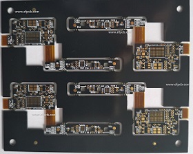 | |
| Related Link: Click here to visit item owner's website (0 hit) | |
| Target State: All States Target City : Shenzhen Last Update : Aug 02, 2023 7:36 AM Number of Views: 107 | Item Owner : Shawn Wang Contact Email: Contact Phone: +86-755-23724206 |
| Friendly reminder: Click here to read some tips. | |
Hot-Web-Ads > Computers > Hardware
© 2024 Hot-Web-Ads.com
USNetAds.com | GetJob.us | CANetAds.com | UKAdsList.com | AUNetAds.com | INNetAds.com | CNNetAds.com | USAOnlineClassifieds.com
2024-05-04 (0.222 sec)