Key Considerations in Multilayer PCB Design (Business Opportunities - Marketing & Sales)
Hot-Web-Ads > Business Opportunities > Marketing & Sales
Item ID 16034239 in Category: Business Opportunities - Marketing & Sales
Key Considerations in Multilayer PCB Design | |
Multilayer PCB design is a critical step in developing compact, high-performance electronic systems. Effective multilayer designs require a strategic balance of electrical, mechanical, and thermal parameters. Below are the key considerations engineers focus on during the design phase. 1. Layer Stack-Up Planning A well-balanced layer stack-up ensures signal integrity, reduces EMI, and improves mechanical stability. Common configurations include: 4-layer boards: Signal – Ground – Power – Signal 6-layer boards: Signal – Ground – Signal – Power – Ground – Signal The arrangement depends on the signal frequency, routing complexity, and product size. 2. Impedance Control Controlled impedance is essential for high-speed signals. Designers calculate trace width, dielectric thickness, and material constants to maintain consistent impedance across transmission lines. Stack-up and trace geometry must be precisely matched to the signal requirements. 3. Via Selection and Placement Multilayer PCBs utilize various via types: Through-hole vias: Most common, connect all layers Blind vias: Connect outer to inner layers Buried vias: Connect internal layers only Microvias: Used in HDI designs for finer routing Proper via planning helps reduce signal loss and optimizes space. 4. Power and Ground Plane Design Dedicated planes reduce ground bounce and provide a low-impedance return path for signals. To minimize noise and improve power delivery, designers ensure planes are continuous, with minimal splits or interruptions. 5. Crosstalk and EMI Management To limit interference, designers: Maintain adequate spacing between traces Use differential pairs with controlled impedance Route signals over solid reference planes Avoid parallel high-speed lines on adjacent layers Signal layers are often adjacent to ground planes to shield noise. 6. Thermal Considerations With more layers and components, heat dissipation becomes a challenge. Designers implement: Thermal vias under heat-generating components Copper pours and heat sinks Even layer distribution to prevent warpage during reflow 7. DFM (Design for Manufacturability) Multilayer designs must meet fabrication limits such as: Minimum trace width and spacing Via aspect ratios Lamination constraints Close collaboration with PCB manufacturers ensures higher yields and fewer production issues. Conclusion Multilayer PCB design demands precision and planning across electrical, mechanical, and thermal domains. A successful design enables high-speed, low-noise performance and ensures reliable operation in complex electronic systems. 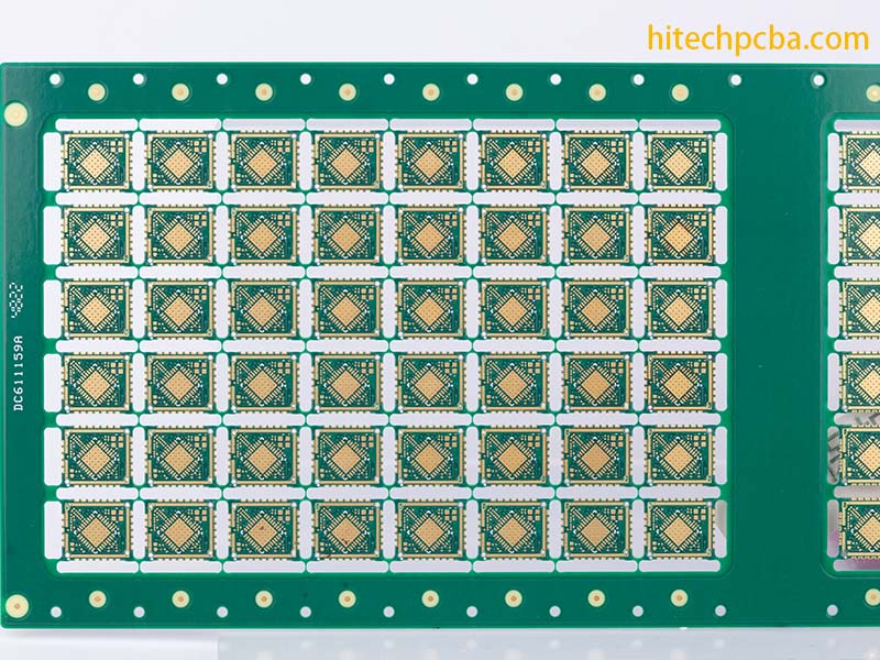 | |
| Target State: All States Target City : All Cities Last Update : May 22, 2025 2:44 AM Number of Views: 48 | Item Owner : Alisa Contact Email: Contact Phone: +86 18126460264 |
| Friendly reminder: Click here to read some tips. | |
Hot-Web-Ads > Business Opportunities > Marketing & Sales
© 2025 Hot-Web-Ads.com
USNetAds.com | GetJob.us | CANetAds.com | UKAdsList.com | AUNetAds.com | INNetAds.com | CNNetAds.com | USAOnlineClassifieds.com
2025-08-20 (0.252 sec)